DPCC™ : Direct Printed Copper on Ceramics base substrate
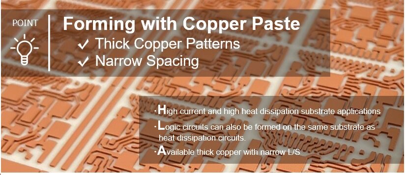
■Feature
① Thickness Over 1,000μm* (* Depends On Printing Condition)
・Thickness suitable for power semiconductor substrates
・Can form areas of different thickness on the same wiring
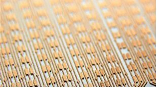
② Pattern spacing Min.25μm* (* Depends On Printing Condition)
・Wiring by screen printing using copper paste
・High-density wiring beyond conventional DBC/AMB etch rules
③ Various Ceramics Substrate
・Available Cu wiring patterns on various ceramic substrates
・AL2O3 , ALN , Si3N4
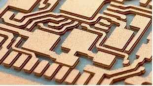
■Shape of wiring
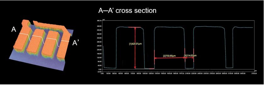
・Good rectangular shape and flatness on surface
・Form L/S that is difficult to achieve with etching method