As high-density mounting progresses, semiconductor components need to be smaller and thinner.
In order to meet the market needs, we have realized the miniaturization and thinning of the package by using the assembly technology specialized for thinness. AOI provide miniature and thin non-lead packages (QFN, DFN).
Feature
- Non-leaded packages(DFN, QFN)
- Thinning of material (Wafer:40μm thickness/ Frame:80μm thickness/ Die attach material thickness:10μm)
- Low loop wire control (40μm)
- Filler thinning high liquidity resin (filler diameter: 20μm)
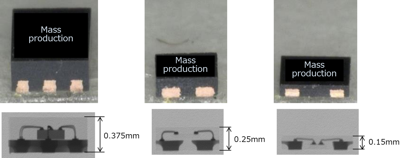
Structure
- Package thickness 0.375mm (Typ): Mass production
- Package thickness 0.25mm (Typ) : Mass production
- Package thickness 0.15mm (Typ) : Mass production
Application
- Sensor
- DC-DC converter, LDO
- Power supply protection IC, etc.