Can provide custom-made products that meet the needs of customers.
- Can propose the optimum package size (width / Length) suitable for the chip.
- Can make proposals with a land design that flexibly responds to customer requests.
- Wafer sizes to 6inch, 8inch, and 12inch are available.
Characteristic (Summary)
- High reliability/High electrical characteristics.
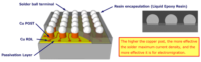
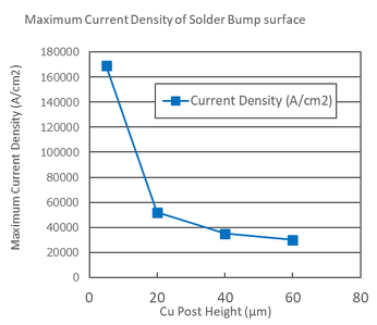
- High current capacity
- Reduce chipping on Circuit side (Protected by resin)
- Improve quality for low-k
- Improve mountability (High precision coplanarity)
- Low temperature process (Damage reduction for insulation film)
| WLP Type | Standard Type | Thin Type |
|---|---|---|
| 1) Solder Terminal Height [μm] | 150 - 250 | 80 (Max.) |
| 2) Cu Post Diameter [μm] | 100 - 250 | |
| 3) Epoxy Thickness [μm] | 50 - 70 | 40 - 50 |
| 4) Cu Redistribution Line / Space [μm] (Min.) | 10 / 10 | |
| 5) PI Thickness [μm] | 4 - 15 | |
| 6) Body Thickness [μm] | 300 - 400 (or higher) | 80 ‐ 300 |

Analog/Power : PMIC/Switch/Converter/GPS/Battery Control/Others
RF/Security : WiFi/LTE 4G/Bluetooth/RFID
Sensor/MEMS : CIS/Compass/Magnetic
Automotive : RF tuner for Navigation system
Memory : DDR/Flash/FCRAM
- Structure and Reliability Details ⇒ Click here